The actual structural design of a photovoltaic device depends on the limitations of the material used in the PV cell. We will look briefly at four basic device designs commonly used with the materials we have discussed .
Crystalline silicon is the primary example of this kind of cell. A single material—crystalline silicon—is altered so that one side is p-type, dominated by positive holes, and the other side is n-type, dominated by negative electrons. The p/n junction is located so that the maximum amount of light is absorbed near it. The free electrons and holes generated by light deep in the silicon diffuse to the p/n junction, then separate to produce a current if the silicon is of sufficient high quality.
In this homojunction design, we may vary several aspects of the cell to increase conversion efficiency:
-
Depth of the p/n junction below the cell's surface
-
Amount and distribution of dopant atoms on either side of the p/n junction
-
Crystallinity and purity of the silicon
Some homojunctions cells have also been designed with the positive and negative electrical contacts on the back of the cell. This geometry eliminates the shadowing caused by the electrical grid on top of the cell. A disadvantage is that the charge carriers, which are mostly generated near the top surface of the cell, must travel farther—all the way to the back of the cell—to reach an electrical contact. To be able to do this, the silicon must be of very high quality, without crystal defects that cause electrons and holes to recombine.
Heterojunction Device
An example of this type of device structure is a CIS cell, where the junction is formed by contacting two different semiconductors—CdS and CuInSe2. This structure is often chosen for producing cells made of thin-film materials that absorb light much better than silicon. The top and bottom layers in a heterojunction device have different roles. The top layer, or "window" layer, is a material with a high bandgap selected for its transparency to light. The window allows almost all incident light to reach the bottom layer, which is a material with low bandgap that readily absorbs light. This light then generates electrons and holes very near the junction, which helps to effectively separate the electrons and holes before they can recombine.
Heterojunction devices have an inherent advantage over homojunction devices, which require materials that can be doped both p- and n-type. Many PV materials can be doped either p-type or n-type, but not both. Again, because heterojunctions don't have this constraint, many promising PV materials can be investigated to produce optimal cells.
Also, a high-bandgap window layer reduces the cell's series resistance. The window material can be made highly conductive, and the thickness can be increased without reducing the transmittance of light. As a result, light-generated electrons can easily flow laterally in the window layer to reach an electrical contact.
p-i-n and n-i-p Devices
Typically, amorphous silicon thin-film cells use a p-i-n structure, whereas CdTe cells use an n-i-p structure. The basic scenario is as follows: A three-layer sandwich is created, with a middle intrinsic (i-type or undoped) layer between an n-type layer and a p-type layer. This geometry sets up an electric field between the p- and n-type regions that stretches across the middle intrinsic resistive region. Light generates free electrons and holes in the intrinsic region, which are then separated by the electric field.
In the p-i-n amorphous silicon (a-Si) cell, the top layer is p-type a-Si, the middle layer is intrinsic silicon, and the bottom layer is n-type a-Si. Amorphous silicon has many atomic-level electrical defects when it is highly conductive. So very little current would flow if an a-Si cell had to depend on diffusion. However, in a p-i-n cell, current flows because the free electrons and holes are generated within the influence of an electric field, rather than having to move toward the field.
In a CdTe cell, the device structure is similar to the a-Si cell, except the order of layers is flipped upside down. Specifically, in a typical CdTe cell, the top layer is p-type cadmium sulfide (CdS), the middle layer is intrinsic CdTe, and the bottom layer is n-type zinc telluride (ZnTe).
Multijunction Devices
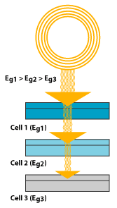
This structure, also called a cascade or tandem cell, can achieve a higher total conversion efficiency by capturing a larger portion of the solar spectrum. In the typical multijunction cell, individual cells with different bandgaps are stacked on top of one another. The individual cells are stacked in such a way that sunlight falls first on the material having the largest bandgap. Photons not absorbed in the first cell are transmitted to the second cell, which then absorbs the higher-energy portion of the remaining solar radiation while remaining transparent to the lower-energy photons. These selective absorption processes continue through to the final cell, which has the smallest bandgap.
A multijunction device is a stack of individual single-junction cells in descending order of bandgap (Eg). The top cell captures the high-energy photons and passes the rest of the photons on to be absorbed by lower-bandgap cells.
A multijunction cell can be made in two different ways. In the mechanical stack approach, two individual solar cells are made independently, one with a high bandgap and one with a lower bandgap. Then the two cells are mechanically stacked, one on top of the other. In the monolithic approach, one complete solar cell is made first, and then the layers for the second cell are grown or deposited directly on the first.
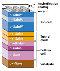
This multijunction device has a top cell of gallium indium phosphide, then a "tunnel junction" to allow the flow of electrons between the cells, and a bottom cell of gallium arsenide.
Much of today's research in multijunction cells focuses on gallium arsenide as one (or all) of the component cells. These cells have efficiencies of more than 35% under concentrated sunlight—which is high for PV devices. Other materials studied for multijunction devices are amorphous silicon and copper indium diselenide
http://www1.eere.energy.gov/solar/solar_cell_structures.html#pin_nip